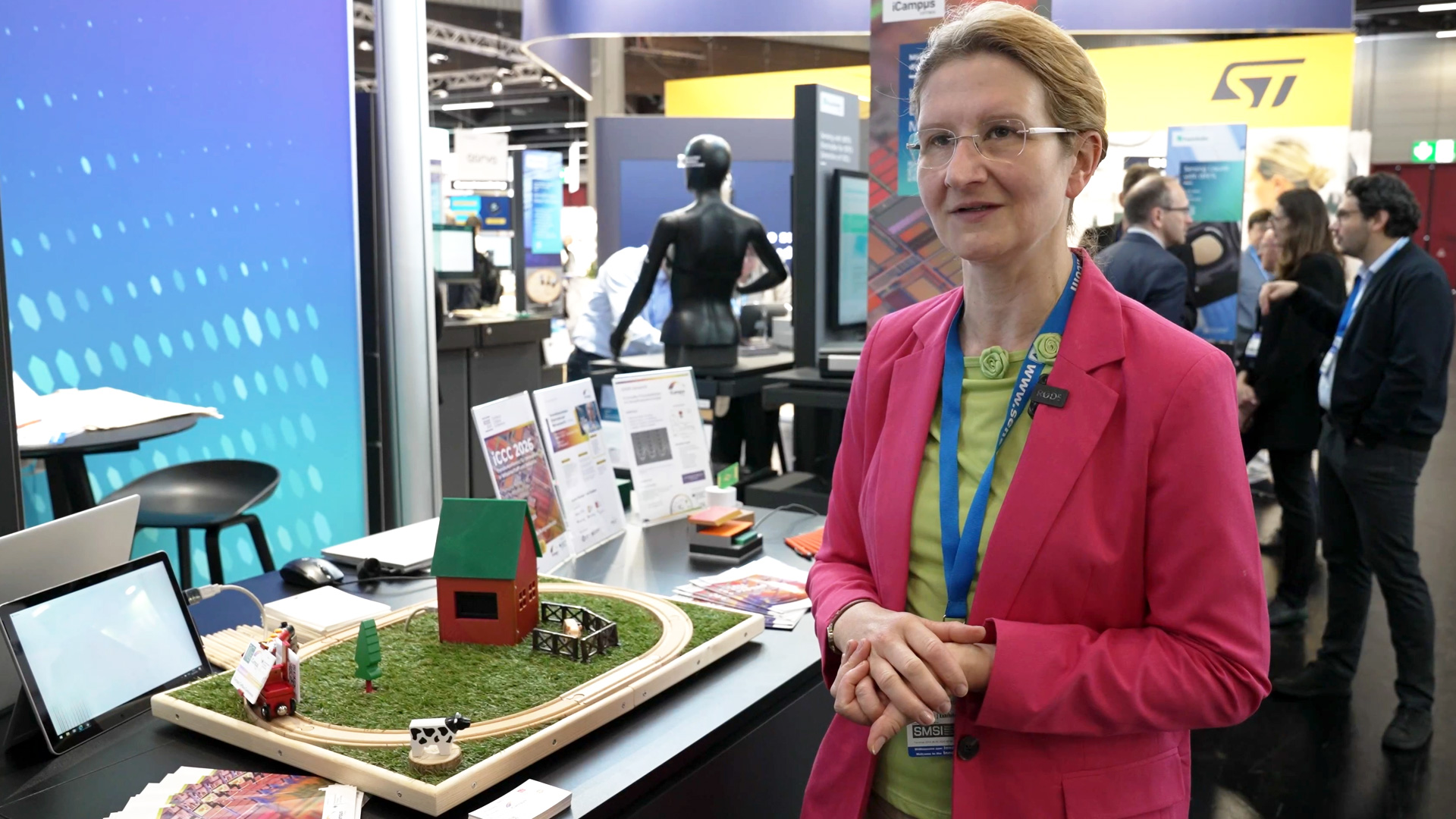
Ultrasonic technology of the future: invisible sensors with a wide range of applications
by A. Bergmeier - 2025-05-07A tiny chip encased in an inconspicuous housing can scan rooms, recognize gestures, and even serve as an acoustic camera. The underlying technology is based on capacitive micromechanical ultrasonic transducers (CMUT), which are setting new standards in contactless sensor technology.


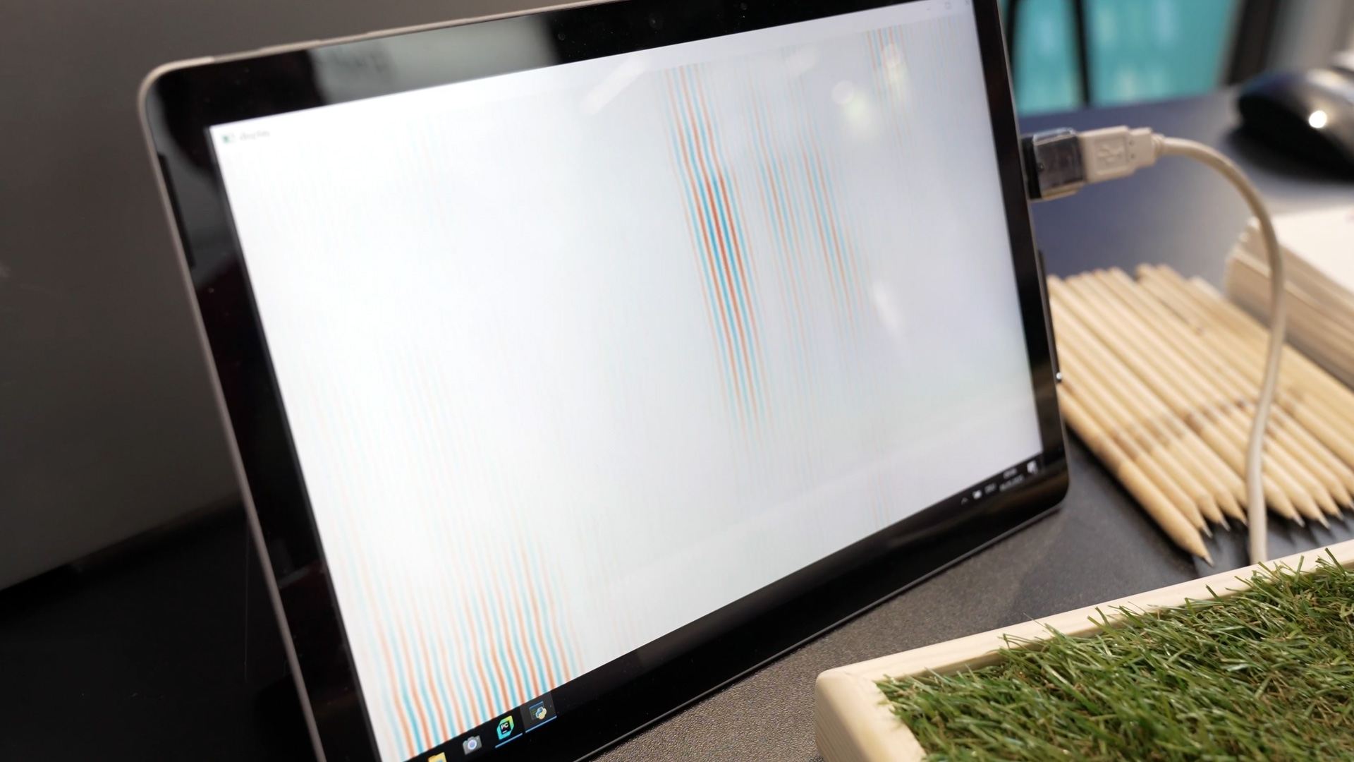
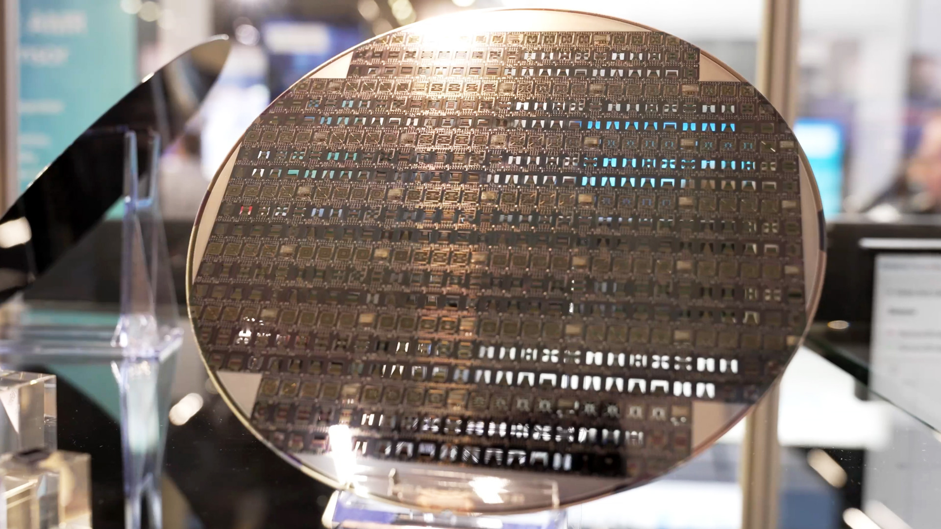
CMUT high-tech sensor for ultrasonic sensor technology in miniature format
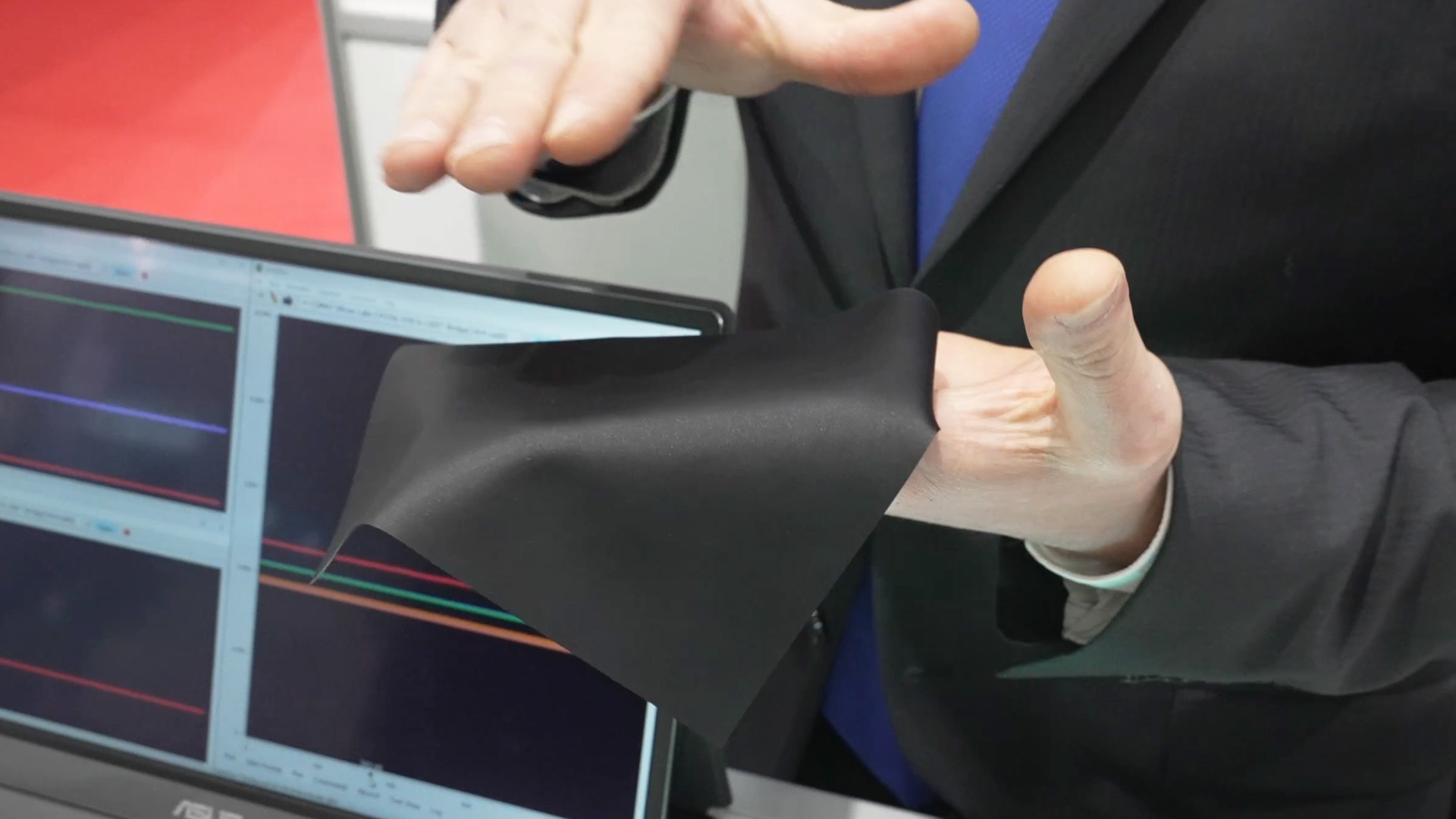
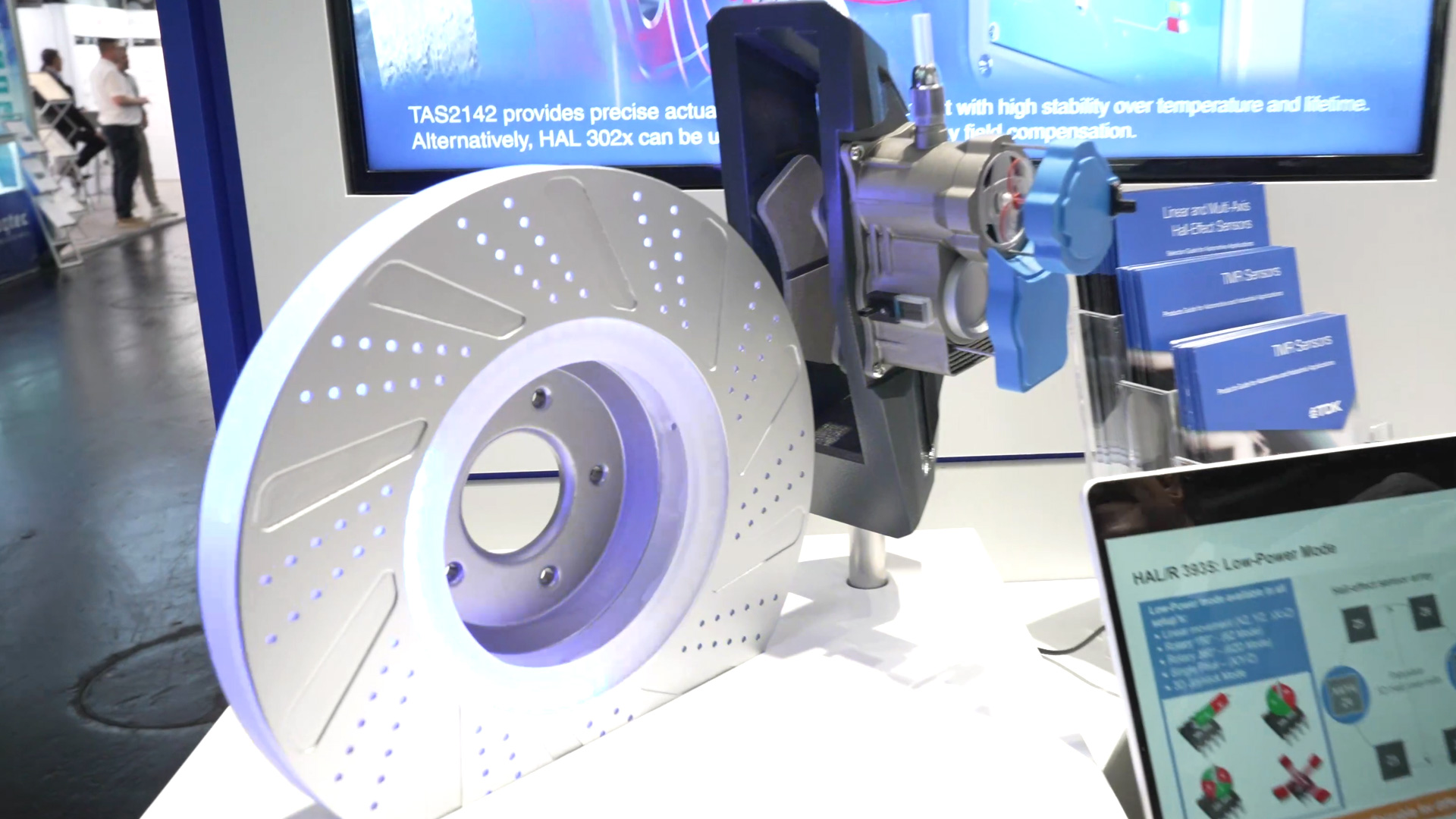
Hidden in a small housing is a capacitive micromechanical ultrasonic transducer – CMUT for short. This technology emits sound waves that are invisible to the human eye, whose reflections are captured and evaluated by the environment. The scenario presented demonstrates how a single chip can be used to detect movements – such as reflections from a passing train or fixed objects such as a tree or a cow. The CMUT enables precise distance measurement, which can be used for environment detection in vehicles or in industry, for example.

Gesture control through sound: touch-free operating concepts
A key area of application for CMUT technology is gesture control. The pandemic has led to a sharp rise in interest in touchless operating concepts, whether in vehicles for controlling the radio or air conditioning, or in public spaces for triggering traffic lights without having to press a button. New possibilities are also opening up in clinical environments: Doors can be opened with simple hand movements without direct contact.
Ultrasound: Acoustic imaging as an alternative to optical cameras
Acoustic sensor technology can serve as a replacement or supplement to optical cameras. Similar to how bats orient themselves in space using echolocation, CMUT also allows acoustic detection of the environment – without the need for light. Special arrays can even be used to display the shape of objects. The goal is to develop 2D cameras based on ultrasound that are robust and insensitive to lighting conditions.
Contactless, low-energy, safe: advantages of CMUT technology
A major advantage of the technology is its inconspicuousness: the sound waves are neither audible nor perceptible to humans, have low energy, and are completely harmless. Even in direct contact—for example, with the hand—there is no physical stimulus. This makes the technology ideal for sensitive applications, such as in medicine or everyday life, where comfort and safety are required.
Resolution down to the millimeter: AI-based object recognition with ultrasonic arrays
The combination of CMUT chips and artificial intelligence opens up new possibilities in the automated recognition of complex scenarios. This allows large areas to be scanned and characteristic patterns to be recognized. The integration of multiple chips in arrays improves spatial resolution, which now extends to around one millimeter. This enables precise surface detection in industrial manufacturing—even where automation solutions are needed due to a shortage of skilled workers.

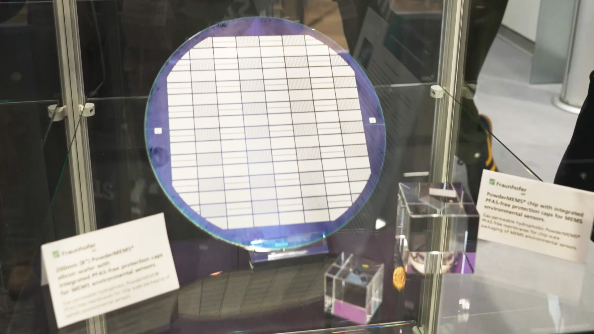
Cost-effectiveness through wafer production and high volumes
CMUTs are manufactured on a wafer basis in batch processes. The preparation work – for lithography masks or process development, for example – is complex, but the production costs per chip are significantly lower for large quantities. In applications such as the automotive sector, where high volumes are required, these sensors can now be manufactured very cost-effectively – in some cases in the sub-cent range, depending on the chip type, materials, and series volume.


Trade fair reporting Germany - Trade fair knowledge, dates & events