MEMS sensor technology for medical technology: Miniaturized pressure and process sensors from our own wafer production
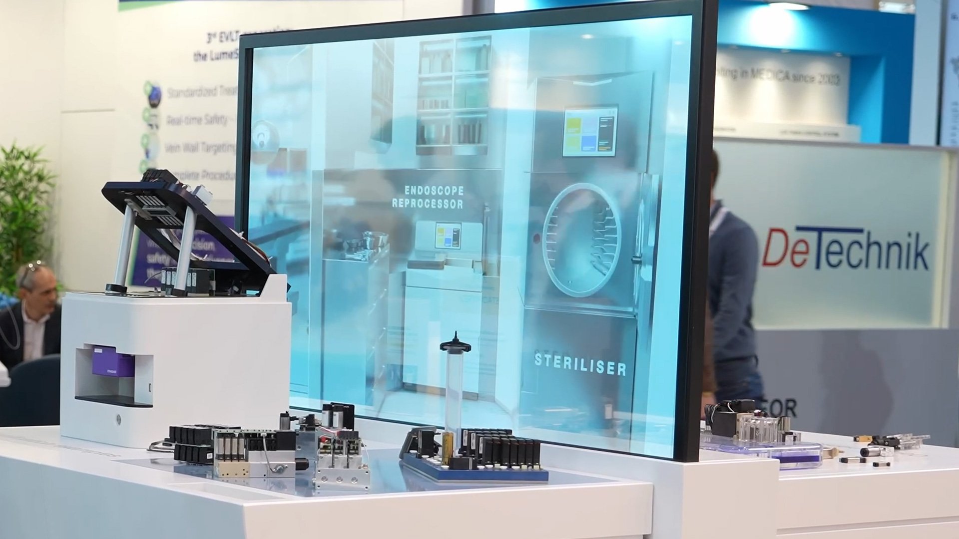
by B. Velonavy - 2025-11-24At Medica, Bürkert is focusing on a new MEMS technology that has been specially developed for compact, high-precision sensor applications. The sensors are based on our own wafer production and, thanks to their size, material selection, and integration capability, can be flexibly integrated into medical devices and disposables. The combination of miniaturization, clean room production, and customer-specific adaptability opens up new possibilities for ventilation, dialysis, in vitro diagnostics, and laboratory technology.

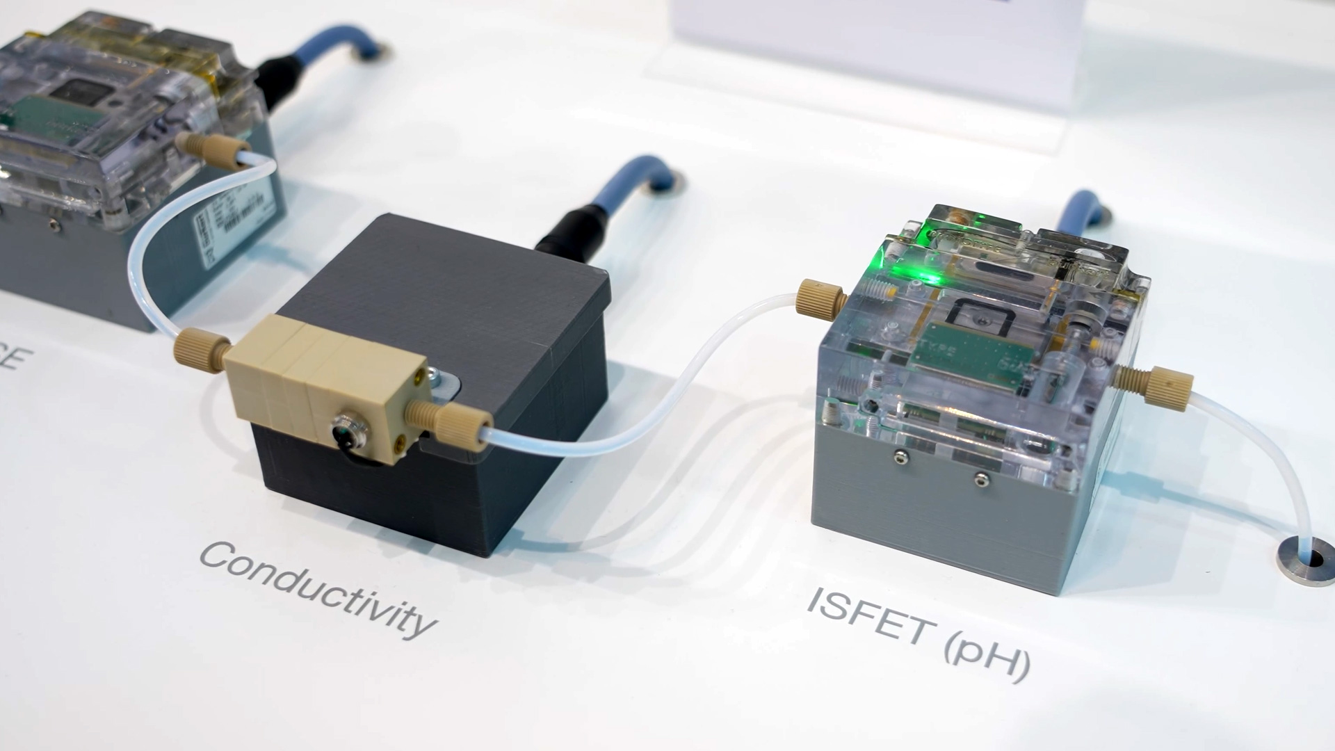
Bürkert MEMS technology for integrable sensor concepts
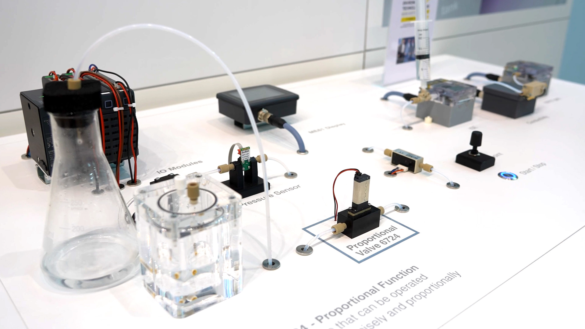
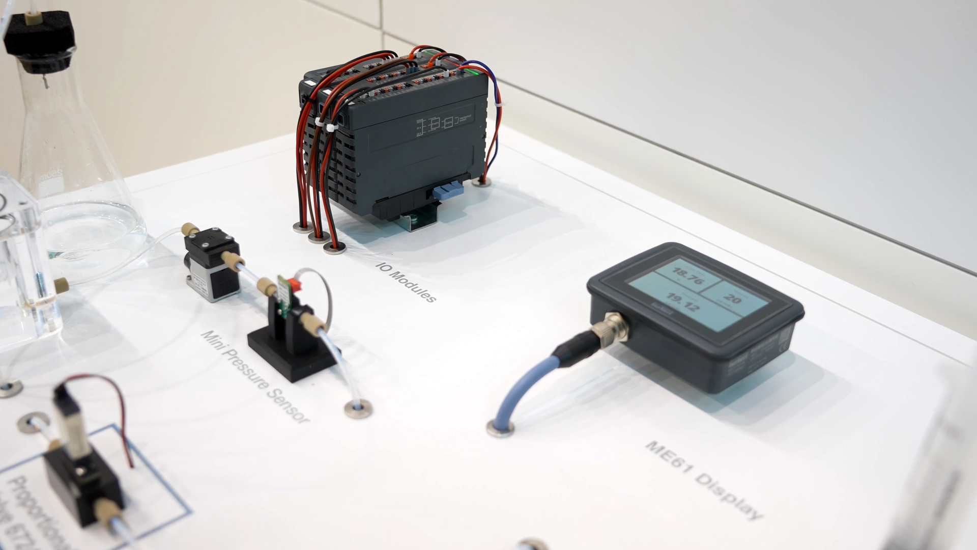
The MEMS technology presented forms the core of a sensor portfolio designed for maximum flexibility. The sensors are extremely small, completely semiconductor-based, and particularly easy to integrate—an advantage that is particularly evident in disposables and space-critical medical systems. A newly developed pressure sensor illustrates this approach: it combines small dimensions with mechanical stability and cost-efficient manufacturing. The architecture consistently supports miniaturization and enables early access to new technologies, for example through evaluation kits for developers, startups, or manufacturers with their own R&D focus.
The technology addresses classic challenges of modern medical technology: limited installation space, increased modularization of devices, growing demand for disposable components, and the need to embed sensor technology in highly complex process cycles. The miniaturization of sensor elements allows for greater design freedom and the development of systems that would have been unwieldy or impossible to construct in previous generations.

Sensors for ventilation, dialysis, and diagnostic systems
MEMS sensors have a wide range of applications. In ventilation technology, fast pressure responses and stable signal quality are essential, which is supported by the semiconductor-based architecture. In dialysis applications, chemical resistance plays an important role, especially for polymer-based sensor elements such as PEEK. In in vitro diagnostics, where small chambers and repeatable measurement conditions are crucial, the compact design enables reliable integration into cartridges or fluidic modules. The sensors are also used in laboratory technology and bioprocess engineering: to determine glucose values, pH measurements, or ion selectivity. These applications require fast response times and high sensitivity, as biological processes are often dynamic and small fluctuations must be detected immediately. MEMS technology helps to precisely map these measurement conditions and embed them in automated analysis systems.
Wafer production for flexible development and customer-specific solutions
A key point of the presentation is the company's own wafer production in a clean room. Bürkert manufactures 100 percent of its sensors in-house, thereby controlling all process steps from raw material to the final sensor element. This vertical manufacturing allows specific customer requirements to be implemented directly, rather than adapting standard components or making compromises. This production structure gives the company influence over design issues, material combinations, sensor geometries, and electrical parameters. Users benefit from tailor-made solutions that precisely reflect their process requirements and shorten time-to-market. At the same time, only the functions that are really needed are included – an advantage in systems where unnecessary complexity increases both costs and validation effort.
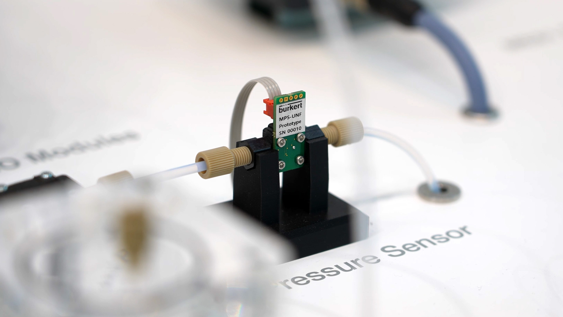
Mini pressure sensor made of PEEK and direct membrane architecture
A particularly innovative example is the mini pressure sensor with a diameter of only three millimeters. Made entirely of PEEK, it is approved for medical applications and is highly resistant to chemicals and heat. Its design differs fundamentally from many competing products: the PEEK membrane itself forms the measuring element and is directly coupled to the electronics. Conventional buffer solutions—such as oil or metal interlayers—are no longer necessary. This results in higher sensitivity and faster response times because the signal does not have to be transmitted through multiple media. The direct membrane technology also prevents attenuation and hysteresis effects that can occur in conventional designs. For medical technology OEMs, this means more stable measurements, fewer deviations, and less calibration effort.
Flexibility in production and economical quantities
The technology is also versatile in series production. The wafers are divided into segments, from which individual sensor housings and membranes are created. This structure allows for a high degree of flexibility in terms of sizes and contours and enables cost-effective production even for smaller quantities. Typical applications range between 500 and 1,000 devices per year—an order of magnitude that is common in many specialized medical applications. At the same time, the technology is scalable for significantly larger production volumes.


Trade fair reporting Germany - Trade fair knowledge, dates & events